Oxide-semiconductor integration
1. Atomically controlled surface passivation
For silicon-oxide interfaces we determined a new PLD-based pathway for components integration. Before the growth, Si substrate needs to be exposed to UHV at elevated temperature to remove the native oxide from its surface which is amorphous and thus limits the crystal quality of the overgrown oxide layer. The resulting surface reconstructs and forms half order streaks in the reflection high-energy electron diffraction (RHEED) pattern for (001)Si. The resulting surface is thermodynamically instable and thus requires corresponding passivation which we successfully performed using metallic strontium. Deposition conditions for controlling the Si surface states using metallic Sr were precisely determined. It was observed that Sr induces a gradual transformation from 2×1 through 2×3 to 1×2 reconstruction, which corresponds to 0, 1/6, and 1/2 ML coverage of Sr, respectively (Fig. 1). We demonstrated experimentally, for the first time, the possibility of preparing such a buffer layer using PLD, which for this method reveals a new path towards epitaxial integration of STO and other functional oxides with Si.1 Based on the results on PLD integration of oxides with Si I was invited with Dr. F. Sanchez to prepare a chapter of a roadmap “Towards Oxide Electronics”, which was recently published in Applied Surface Science.2
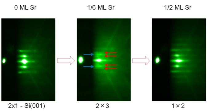
Figure 1: Evolution of RHEED pattern in [110] azimuth for Si surface reconstruction, which changes during the deposition of metallic Sr from 2x1 for pure silicon to 1x2 for ½ monolayer coverage of Sr, which corresponds to SrSi2.
2. In situ STM analysis
Due to high reactivity of Si surface, we determined its atomic characteristics by in-situ scanning tunnelling microscope (STM). In our study we analysed surface of reconstructed (001)Si, as well as the surface buffered with Sr, which was prepared from ½ ML of Sr and serves as a template for growth with STO. Samples were transferred into STM chamber in UHV using a suitcase. STM results demonstrated considerable difference of surface morphology between reconstructed Si and the buffer layer, which is due to complete transfer of topmost Si atoms towards step edges as ½ ML of Sr was deposited on Si substrate. The STM images reveal an atomically ordered surface with terraces composed of one-dimensional (1D) chains running along perpendicular directions on neighbouring terraces. The 1D chains are separated by 0.78 nm and exhibit a low-amplitude corrugation with a period of 0.39 nm. The measured values agree well with the size of the 1×2 unit cell observed for similar MBE-grown surfaces, while the density of the surface defects is somewhat higher in the PLD case. According to simulated STM images based on DFT calculations, two types of surface defects were identified and explored: arrays of Sr vacancies and Sr adatoms.3
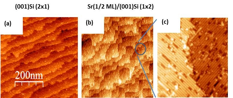
Figure 2: STM image of Si surface, before and after the deposition of ½ ML of metallic Sr, which causes its reconstruction to change from 2x1 to 1x2 (a and b, respectively). Magnified image revels increased defect concentration for the buffer layer related to energetics of PLD plume (c).
3. SrO-induced surface deoxidation
The application of metallic Sr is industrially inappropriate since the target requires oxygen- and moisture-free handling and is thus hard to realize. For these reasons we investigated the applicability of the chemically much more stable SrO in the process of native-oxide removal and Si-surface stabilization using the PLD technique with process parameters, which are acceptable in industrial applications. We deposited SrO over Si/SiO2 in a vacuum and applied different annealing conditions, with the temperature ranging up to 850 °C. Because the deposition took place in a vacuum, a multilayer composed of SrO, Sr-silicate, modified Si, and Si as a substrate was initially formed according to our X-ray reflectivity and X-ray photoelectron spectroscopy measurements. It was observed that during the subsequent annealing the topmost layer epitaxially orders in the form of islands, while a further increase in the annealing temperature induced rapid desorption and surface deoxidation, leading to a 2×1 Sr-reconstructed Si surface. This process description was supported by RHEED and is schematically presented in Fig. 3. Since the reconstruction is accompanied by distinctive surface roughening, the experimental conditions must be carefully optimized to minimize the effect. For different process atmospheres we also investigated deoxidation temperature and time for occurrence of Si reconstruction, as well as the coherence length of obtained 2×1 streaks. It was observed that deoxidation temperature and the vacuum can be effectively decreased to 740°C and to 10-7 mbar, respectively, while maintaining the quality of the surface structure.4,5
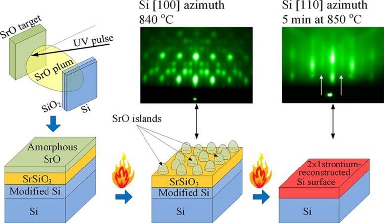
Figure 3: Schematics of SrO-induced surface deoxidation and reconstruction using the PLD technique.4
4. STO growth on Si substrates
On a Sr-passivated Si substrate we grew STO in a two-step procedure. In the first step the so-called “kinetically controlled sequential deposition (KCSD)” method was applied to deposit a 15 unit-cell thick protective STO layer. A detailed analysis of initial deposition parameters was performed, which enabled us to develop a complete protocol for integration, taking into account the peculiarities of the PLD growth, STO critical thickness, and process thermal budget, in order to kinetically trap the reaction between STO and Si and thus to minimize the thickness of the interface layer. The rest of STO was grown in the second step of the procedure at elevated temperature in a continuous way. The as-prepared oxide layer is monocrystalline and exhibits STO(001)||Si(001) out-of-plane and STO[110]||Si[100] in-plane orientation.6,7,8
5. PMN-PT growth on STO substrates
We investigated the PLD growth of Pb(Mg1/3Nb2/3)O3-PbTiO3 (PMN-PT) on non-conductive STO, rendering them appropriate for use in longitudinal (d33)-mode energy harvesters, after being integrated with Si platform. Through our comprehensive approach we were able to effectively compensate for the loss of Pb occurring during the growth, thereby controlling the phase composition of the thin films. We found that, in order to achieve pure perovskite growth at optimal deposition parameters, over 15 mol.% of PbO excess were necessary. In case growth of PMN-PT commences from LaNiO3, which act as electrode layers, lead compensation is not needed due to material`s different surface chemistry. However, as-prepared heterostructures can only be used in transverse (d31)-mode of operation with smaller figure of merit of energy-harvesting device.9
REFERENCES:
1 D. Klement, M. Spreitzer, and D. Suvorov, Applied Physics Letters, 106, 071602, 2015. ARTICLE DOWNLOAD
2 M. Coll et al., Applied Surface Science, 482, 1, 2019. ARTICLE DOWNLOAD
3 T. Parkelj, E. Zupanič, W.Y. Tong, E. Bousquet, D.D. Fernandez, G. Koster, P. Ghosez, M. Spreitzer, Applied Surface Science, 471, 664, 2019. ARTICLE DOWNLOAD
4 Z. Jovanović, M. Spreitzer, J. Kovač, D. Klement, and D. Suvorov, ACS Applied Materials & Interfaces, 6, 18205, 2014. ARTICLE DOWNLOAD
5 Z. Jovanović, M. Spreitzer, U. Gabor, and D. Suvorov, RSC Advances, 85, 82150, 2016. ARTICLE DOWNLOAD
6 D. Diaz-Fernandez, M. Spreitzer, T. Parkelj, J. Kovač, D. Suvorov, RSC Advances, 85, 82150, 2016. ARTICLE DOWNLOAD
7 D. Diaz-Fernandez, M. Spreitzer, T. Parkelj, D. Suvorov, Applied Surface Science, 455, 227, 2018 ARTICLE DOWNLOAD
8 M. Spreitzer, D. Klement, J. Kovač, R. Egoavil, J. Verbeeck, A. Založnik, G. Koster, G.V. Tendeloo, D. Suvorov, G. Rijnders, under review, Journal of Materials Chemistry C. ARTICLE DOWNLOAD
9 U. Gabor, M. Spreitzer, W.J. Wu, D. Suvorov, Journal of the European Ceramic Society, 38, 4453, 2018. ARTICLE DOWNLOAD