Nanoparticles and Thin Films for Photocatalytic and Photoelectrochemical Water Splitting
1. Background and state-of-the-art
The conversion of solar energy in to hydrogen by means of photocatalytic (PC) and photoelectrochemical (PEC) water splitting has been recently recognized as promising strategy for producing of renewable energy. Both approaches are based on the same mechanism and impose the same thermodynamic and kinetic requirements to involved semiconductor materials. In contrast to PEC, where evolved H2 and O2 are separated due to their evolution on different photoelectrodes, in PC a mixture of H2 and O2 are obtained since water splitting reaction takes place in the suspension of photocatalysts particles. The main disadvantages of PC with respect to PEC are related to the costs for H2 and O2 separation and reduced H2 yield due to the thermodynamically favourable backward reaction. However, the PC is regarded as the cheapest approach and offers several advantages including possibility for easy increase of photocatalysts’ effective surface area and no need for electrical connection. Additionally, in dual-functional photocatalysis H2 evolution can be combined with oxidative degradation of toxic organic compound or some other oxidation reaction, enabling formation of added-value products.1
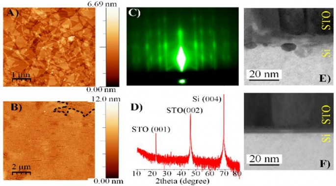
Figure 1: AFM images of GO layers spin-coated on Si/SiO2 substrate before (A) and after (B) STO deposition using lab. PLD (100 nm). RHEED (C) and XRD (D) patterns of STO grown on SrO/rGO/Si surface. The interface between STO and silicon with (F) and without (E) rGO. Dashed line in (B) show region with 1-monolayer thick GO.
In spite of the high promises of PC and PEC, several challenges and issues related to the efficiency of solar light absorption, costs, stability and sustainability have to be solved that both processes become economically viable for H2 production. Progress in the fields can be made by designing of new systems, materials and interfaces based on the understanding of the interfacial phenomena, thermodynamic and kinetics criteria. In the development of PEC cells, the integration of narrow band-gap semiconductors (Si, Ge, GaAs) with thin metal oxide protective layer has recently attracted great scientific attention. 2,3,4 Si, Ge, GaAs semiconductors, which are characterized by good absorption of the visible and infrared part of the solar light, high electron-hole mobilities and conduction band (CB) energy more negative than hydrogen redox (EH+/H2) potential, are not chemically stable in the relevant solution environments during long term operations. The protection of the semiconductor against corrosion can be achieved by the epitaxially grown protective oxide material with good lattice match with the semiconductor and appropriate conduction band alignment that facilitate electron transport and reduce the recombination at the interface. Si is a narrow band gap semiconductor (1.1 eV) and exhibit (001) surface unit cell (3.84 Å) that matches well with the lattice constant of a cubic perovskite SrTiO3 (STO) (3.905 Å).2 Additionally, the STO/Si heterojunction is characterized by nearly zero conduction-band offset. Although STO was proved as appropriate protective oxide layer for Si-based photocatode for PEC H2 evolution, there are still unresolved issues related to the influence of the STO/Si interface and characteristics of the epitaxial STO layer on the solar-to-hydrogen (STH) efficiency. We propose a radically new approach for controlling of the interface between semiconductor (i.e. Si) and protective oxide layer (i. e. STO) by graphene oxide (GO), that enables remote epitaxial growth of STO on Si substrate (Figure 1). Insertion of graphene oxide between STO and Si was found to result in sharp, atomically defined interface.
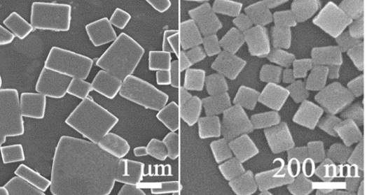
Figure 2: Scanning electron microscope (SEM) images of ferroelectric (001) oriented BaTiO3 plates (left) and nanoblocks (right), prepared by topochemical conversion from Bi4Ti3O12 plates (Source: M. Maček Kržmanc, Cryst. Growth Des. 17 (2017) 3210).
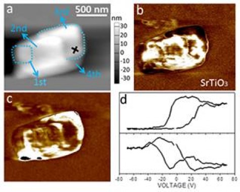
Figure 3: Ferroelectric characteristics of the BaTiO3 nanoblocks (4-nanoblocks assembly): (a) Topography (height image), PFM out-of-plane (b) amplitude and (c) phase images, (d) Local hysteresis loops: amplitude (below) and phase (above) measured in the spot marked with a cross in Fig. (a). (Source: M. Maček Kržmanc et al. Cryst. Growth Des. 17 (2017) 3210-3220.31).
Like in PEC, the efficiency of PC depends on controlling of all steps in the (photocatalytic) process, that are: (i) photon absorption, (ii) photoexcited charge (electron (e-) and hole (h+) separation, (iii) charge diffusion and transport, (iv) catalytic reaction on the catalyst’s active site, and (v) mass transfer.5 Promotion of each step has to be considered in designing of highly effective photocatalyst particles. The basic thermodynamic requirement that has to meet each water-splitting photocatalyst are suitable band gap (>1,23 eV, preferably 1.6-2.4 eV)6, CB more negative than water reduction potential ((H+/H2; 0-0.059 pH, V versus NHE) and valence band (VB) more positive than water oxidation potential (H2O/O2; 1,23-0.059 pH, V versus NHE).7 In our research we focus on engineering of water-splitting photocatalysts based on MTiO3 (M=Sr, Ba, Ca) perovskite particles (Figures 2-6), that meet the aforementioned thermodynamic requirements and concomitantly offer several possibilities for tailoring of chemical compositions, defects and morphologies. In designing of efficient water-splitting photocatalyst particles special attention is paid to enhancement of light absorption by narrowing of the band gap through doping, defects (i.e. oxygen vacancies (Ov)), creation of heterojunctions (i.e. SrTiO3/TiO2, MTiO3/Bi4Ti3O12) and improvement of light harvesting ability by fabrication of hierarchical microporous and mesoporous architectures. For diminishing of e- and h+ recombination we propose exploiting of the internal electric fields, arising in the photocatalyst particle due to ferroelectricity (Figure 3), different facets polarities resulting from different orientations/terminations.8 In the particles with different types of exposed facets several mechanisms can also co-exist and collectively contribute to the formation of differently charged surfaces. In particular, the ferroelectricity in the particles creates relatively strong internal electric field, that separate e- and h+, and also influence the adsorption characteristics of the surface for reactant molecules.9 Our aim is to explore the contribution of these mechanisms to selective spatial reactivity of the particles’ surfaces and to improvement of the STH efficiency.
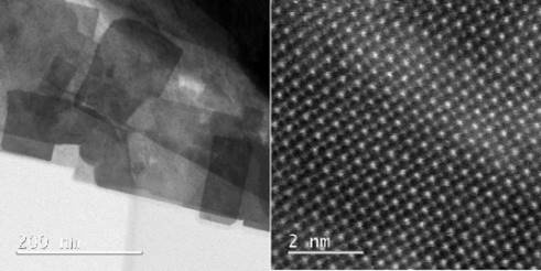
Figure 4: STEM image (left) and high resolution (HR) STEM image (right) of a part of a (100) oriented mesocrystalline SrTiO3 plate.
2. Objectives, originality and impact on new research approaches
In the field of PEC the main objectives are:
(i) To understand key parameters for higher STH efficiency on atomically defined oxide-semiconductor heterostructures.
(ii) To scan for novel protective oxides with engineered band offset and to maximize STH values after their integration with semiconductor photoelectrodes.
(iii) Integration of oxide layer with semiconductor using pulse-laser deposition (PLD).
Our group already developed new approach for successful epitaxial integration of STO on Si using PLD.10,11 Additionally, we also demonstrated that GO nanosheets can effectively direct the growth of STO on Si- substrate (Figure 1). The concept of applying GO as an integration-enabling agent is radically new, fully scalable and will enable a breakthrough for the forthcoming hydrogen economy. The results are anticipated to bring a significant advancement in the understanding of the influence of interface and epitaxial oxide-layer characteristics on STH efficiency.
In the field of PC the main objectives are:
(i) Developing the strategy for controlling the shape, preferential orientation, ferroelectric polarization, type of exposed facets, termination of various perovskite-based particles, including (nano)cubes, (nano)plates, polyhedral micro(nano) crystals, and/or mesocrystalline and heterostructural particles (Figures 2,4-6).
(ii) Defect engineering (Ov) of developed particles.
(iii) Assessment of the photocatalytic performance of the perovskite particles for H2 evolution and evaluation of the contribution of particular aspects (i.e. ferroelectricity, spatial selective photochemical reactivity (different facets/polarities)) to the enhanced photocatalytic performance (in cooperation with the projects partners).
Based on the thorough studies of crystal growth and reaction mechanisms we have already developed several procedures for controlling of perovskite particles morphologies and heterostructures (Figures 2,4-6).12-16
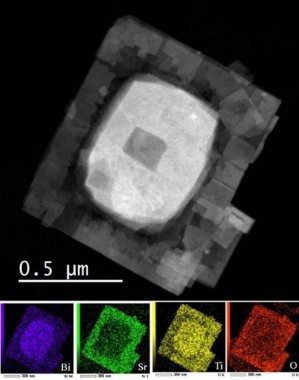
Figure 5: STEM image of SrTiO3/Bi4Ti3O12 heterostructural plate (Bi4Ti3O12 inside, SrTiO3 outer part of the plate).
3. Unique methodology
Attainment of full epitaxy using PLD requires careful monitoring and studies of the film growth and interfaces. In addition to reflection high-energy electron diffraction (RHEED), which is used during film growth, the films are characterized by XPS, Joule-Thomson scanning tunneling microscope. The composition and structural properties of the films are analyzed using Rutherford back-scattering spectrometry, aberration-corrected scanning transmission electron microscope, and high-resolution X-ray diffractometer suited for thin-film studies. Raman spectroscopy are used in operando to determine structural variations of strain engineered films during H2 evolution reaction.
The syntheses of pre-defined perovskite particles morphologies include topochemical conversions of templates or modification of the crystal facets’ energy by additives, which selectively adsorb on particular facets and retard their growth-rate. Information about the type of exposed facets and termination will be obtained by High-Angle Annular Dark-Field Scanning Transmission Electron Microscope (HAADF-STEM), XPS, Time of Flight–Secondary Ion Mass spectrometry (ToF-SIMS). In an event these techniques do not provide straightforward result of surface termination, employing of Low Energy Ion Scattering (LEIS) analysis. Characterization of electronic nature of crystal defects are performed by Electron Energy Loss Spectroscopy (EELS), Photoluminiscence (PL) and electron paramagnetic resonance (EPR).
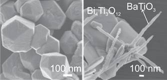
Figure 6: Polyhedral BaTiO3 particles (left) and ferroelectric heterostructure of BaTiO3 nanorods/Bi4Ti3O12 plate (right).
REFERENCES:
1 Kampouri, S., et al.; ACS Catal 9 (2019) 4247-70.
2 Ji, L., et al.; Nat. Nanotechnol. 10 (2015) 84-90.
3 Stoerzinger, K.A., et al.; MRS Communications 8 (2018) 446-52.
4 Kornblum, L., et al.; Energy Environ. Sci. 10 (2017) 377-82.
5 Afroz, K., et al.; J Mater Chem A 6 (2018) 21696-718.
6 Zhao, Y., et al.; Nano Energy 30 (2016) 728-44.
7 Chen, S.S., et al.; Nat. Rev. Mater. 2 (2017) 17.
8 Zhu, Y.S., et al.;Phys. Chem. Chem. Phys. 19 (2017) 7910-18.
9 Cui, Y., et al.; Chem Mater. 25 (2013) 4215-4223.
10 Klement, D., et al.; Appl. Phys. Lett. 106 (2015) 071602. ARTICLE DOWNLOAD
11 Diaz-Fernandez, D., et al.; RSC Advances 7 (2017) 24709-17. ARTICLE DOWNLOAD
12 Maček Kržmanc, M., et al.; Cryst. Growth Des. 17 (2017) 3210-3220. ARTICLE DOWNLOAD
13 Maček Kržmanc, M., et al.; Ceram. Int. 41 (10) (2016) 15128-15137. ARTICLE DOWNLOAD
14 Maček Kržmanc, M., et al.; J. Am. Ceram. Soc. 96 (2013) 3401-3409. ARTICLE DOWNLOAD
15 Maček Kržmanc, M., et al.; Ceram. Int. 44 (2018) 21406-21414. ARTICLE DOWNLOAD
16 Čontala, A., et al.; Acta Chim. Slov., 65(2018) 630-637. ARTICLE DOWNLOAD